Recently, the University of St Andrews unveiled a breakthrough in holographic display technology that may reshape smart devices, communications, gaming, and the entertainment industry in the future.
In a study published in the journal Light: Science & Applications, researchers from the university’s School of Physics and Astronomy combined holographic metasurfaces (HMs) with organic light-emitting diodes (OLEDs) to develop a novel optoelectronic device.
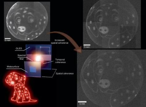
Image source: Light: Science and Applications
Previously, hologram production relied heavily on laser technology. However, the research team discovered that integrating OLEDs with holographic metasurfaces not only simplifies the manufacturing process and reduces device size but also holds the potential for lower costs and broader adoption. This breakthrough successfully addresses the core challenges hindering the widespread use of holographic technology.
The article notes that OLEDs are thin-film devices already widely used in creating color pixels for smartphone screens and certain televisions. As a planar surface light source, OLEDs are also emerging in fields such as optical wireless communication, biophotonics, and sensing. Their high compatibility with other technologies makes them ideal for building miniaturized light-based platforms.
Holographic metasurfaces consist of thin planar arrays of “meta-atoms,” each approximately one-thousandth the diameter of a human hair. These structures are specifically designed to manipulate light properties and can be used to create holograms, with applications spanning data storage, anti-counterfeiting, optical displays, high-numerical-aperture lenses (e.g., for optical microscopy), and sensing.
This study marks the first time these two technologies have been combined to create a fundamental component for holographic displays.
The researchers found that by meticulously designing the shape of each “meta-atom” to control the properties of light passing through it, each meta-atom can function as a “pixel” of the holographic metasurface. As light traverses the metasurface, its properties are subtly altered at each pixel location.
By leveraging these property changes and applying the principles of light interference (where light waves interact to form complex patterns), a pre-designed image can be projected on the opposite side of the metasurface.
Professor Ifor Samuel from the School of Physics and Astronomy remarked, “We are excited to pioneer this new direction for OLED technology. Combining OLEDs with metasurfaces also offers a fresh approach to hologram generation and light manipulation.”
Professor Andrea Di Falco, a Nanophotonics Professor at the same school, noted, “Holographic metasurfaces are among the most versatile platforms for controlling light properties. With this research, we have overcome a key technical barrier that previously prevented metasurfaces from being used in everyday applications. This breakthrough will drive the evolution of holographic display architectures and bring significant advancements to emerging fields such as virtual reality and augmented reality.”
Professor Graham Turnbull, also from the school, added, “While conventional OLED displays require thousands of pixels to render a simple image, this new method can project a complete image using just a single OLED pixel.”
Prior to this development, researchers could only use OLEDs to generate extremely simple graphics, limiting their application in certain scenarios. This breakthrough paves the way for the development of miniaturized, highly integrated metasurface displays. (Source: IT Home)
(Reprinted from www.ledinside.cn)